Core Technology
 Your current location: Home > Thin film prepa...
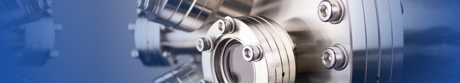
 Physical epitaxy is an advanced technology for preparing material films. It heats solid materials in a vacuum or low-pressure environment, converts them directly into a gas phase, and then deposits them onto the substrate surface to form epitaxial films. This field covers a variety of technologies, including molecular beam epitaxy, magnetron sputtering, and cleavage coating based on molecular beam epitaxy.
Physical epitaxy technology is suitable for epitaxial growth of compound semiconductor films, alloy films, oxide films, and passivation layers, and is widely used in semiconductor device manufacturing, optoelectronics, and lasers.

Fermion Instrument takes the simulation of underlying physical principles as its core technology, including direct Monte Carlo source furnace beam simulation and substrate heater and source furnace thermal field simulation based on full physical quantities.
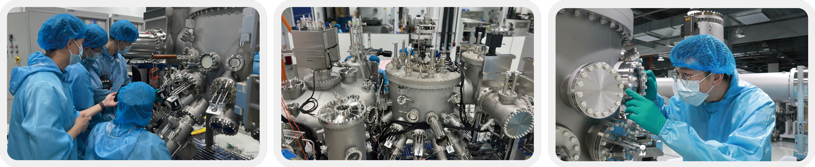
Based on this simulation technology, we have successfully independently developed molecular beam epitaxy, magnetron sputtering and cleavage coating equipment suitable for production lines. Our original large-capacity source furnace, large-size substrate heater, valve cracking source, high-throughput RF plasma source, fully automatic sample transfer robot and other core components have leading technical advantages and have obtained multiple invention patents.
In addition, we are committed to developing the latest epitaxial substrate technology, including silicon-based silicon carbide composite substrates based on atomic replacement technology, and plasma substrate polishing technology suitable for silicon carbide, diamond and other substrates. The silicon-based silicon carbide composite substrate has completed the prototype construction and debugging and small-batch 3-inch substrate production, providing high-quality, low-cost epitaxial substrate alternatives for wide bandgap devices such as gallium nitride and gallium oxide, and solving the incompatibility problem between silicon carbide substrates and CMOS processes, which is suitable for new devices such as silicon photonics.
In terms of molecular beam epitaxy, we have the ability to supply a full range of molecular beam epitaxy complete machines and core components. Currently, we have achieved the sales of single-chip 3-inch, single-chip 4-inch, single-chip 8-inch and multi-chip 3- and 4-inch molecular beam epitaxy complete machines, and have passed the epitaxy process verification and are applied to the epitaxy of traditional materials such as GaAs and InP, as well as the epitaxy of new materials such as GaN and Ga2O3. We also provide core components such as furnace sources, cracking sources, and substrate heaters, which are compatible with users' existing systems, and provide customized system development for new materials and devices such as quantum devices.
The compound interface processing and passivation equipment developed based on molecular beam epitaxy technology can realize the cavity surface processing and passivation of laser bars, breaking through the domestic bottleneck. Since the project development was launched in 2020, more than 10 complete equipment have been sold, promoting the mass production of domestic laser bar chips. During the equipment development process, we not only overcame the technical difficulties of vacuum cleavage, but also launched a self-developed high-throughput H atom source based on plasma technology to provide users with more efficient cavity surface treatment methods. This technology can not only be used for cavity surface cleaning of laser bars, but also for key interface treatment in other microstructures such as Micro-LEDs, and has broad application prospects in compound semiconductor device processes.

PV-200C fully automatic magnetron production line provides solutions for multi-cavity material growth. Typical applications include magnetic tunnel junction and spin logic devices (GMR, TMR, MRAM), microelectromechanical systems (MEMS), organic light-emitting devices (OLED), and solar cells (PV, OPV).
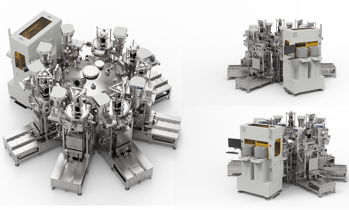
PV-200C can realize multi-cavity interconnection, and the substrate does not need to be exposed to the atmosphere, and the process can be completed in a vacuum.
PV-200C has the ability to automatically process one substrate at a time in sequence or process substrates in parallel to improve production efficiency. Substrate tracking and full process data recording can be achieved.
Fermi magnetron software has a good human-computer interaction interface. Users can customize process recipes, various sensors and vacuum interlocks to ensure efficient and safe operation of the equipment.
In the past ten years of development, we have accumulated rich experience in full-process production management and have a professional after-sales service team, which has won high recognition and firm trust from many customers at home and abroad. In recent years, the company has successfully attracted multiple rounds of financing and has a solid financial strength to provide comprehensive support and guarantee for the company's project development and long-term operation.
In the future, Fermion Instruments will continue to adhere to the customer-oriented and quality-first service principles, provide customers with excellent equipment and products, and create more value!

 中文
中文 021-6525 3206